LTC4242
19
4242f
APPLICATIO S I FOR ATIO
U
U
U
In system board applications, large bypass capacitors
(e10礔) are recommended at each of the system input
supplies to minimize supply glitches as a result of large
inrush or fault currents.
It is important to put C1, the bypass capacitor for the V
CC
pin as close as possible between the V
CC
and GND pins.
Design Example
Consider a PCI Express Hot Swap application example
with the following power supply requirements:
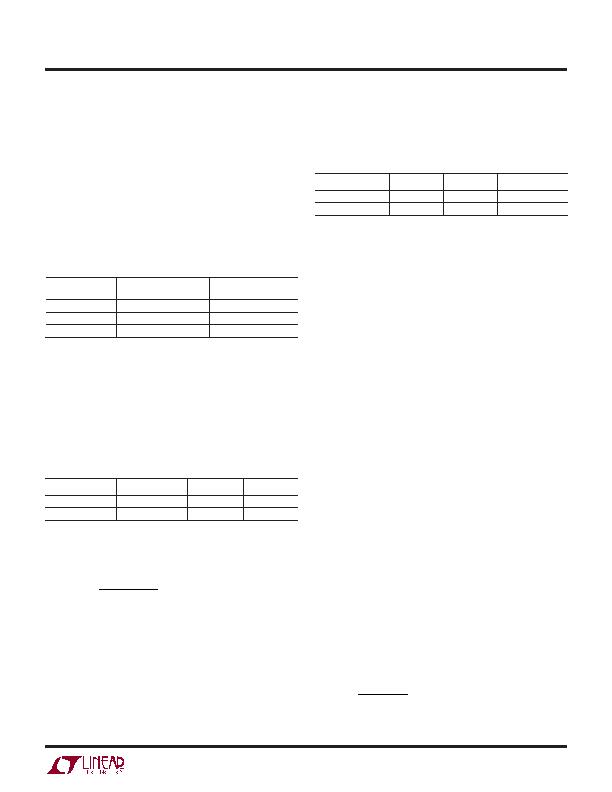
Table 1. PCI Express Power Supply Requirements
SUPPLY VOLTAGE
MAXIMUM SUPPLY
CURRENT
MAXIMUM LOAD
CAPACITANCE
12V
5.5A
2000礔
3.3V
3.0A
1000礔
3.3V
AUX
375mA
150礔
1. Select an R
SENSE
value for each supply. Calculate the
R
SENSE
value based on the maximum load current and the
lower circuit breaker threshold limit, 擵
SENSE(CB)(MIN)
. In
a PCI Express connector, ve pins are allocated for the
12V supply, three pins for the 3.3V supply and one pin for
3.3V
AUX
. The current rating of a connector pin is 1.1A. If
a 1% tolerance is assumed for the sense resistors, then
the following values of resistances should suf ce:
Table 2. Sense Resistance Values
VOLTAGE SUPPLY
R
SENSE
(1%)
I
TRIP(MIN)
I
TRIP(MAX)
12V
8m?/DIV>
5.6A
6.9A
3.3V
13m?/DIV>
3.4A
4.3A
2. Assume no load current at start-up and the inrush current
charges the load capacitance. Compute gate capacitance
with:
C
I
t
V
GATE
GATE UP
OUT
=
( )
"
1
(2)
t
1
is the time to charge up the load capacitor.
With I
GATE(UP)(MAX)
= 13礎 and t
1
= 10ms:
a. For 12V Supply, C
GATE
= 11nF
b. For 3.3V Supply, C
GATE
= 39nF
So a value of 15nF and 47nF (?0%) should suf ce for
the 12V and 3.3V supplies respectively. The worst-case
t
1
and inrush currents are tabulated in Table 3.
Table 3. Worst-Case t
1
and Inrush Current
VOLTAGE SUPPLY
t
1(MIN)
t
1(MAX)
MAX I
INRUSH
12V
13ms
40ms
2.4A
3.3V
11ms
34ms
0.4A
For the internal switch, the slew rate (SR) at the 3.3V
AUX
supply output is limited to 1.7V/ms max. The inrush cur-
rent can then be calculated according to:
I
INRUSH(MAX)
= C
LOAD
" SR
MAX
(3)
The inrush current must be lower than 385mA (I
CBAUX(MIN)
)
for proper start-up. Assuming a tolerance of 30% for the
load capacitance, the value of C
LOAD
should not exceed
170礔.
3. Next is the selection of MOSFETs for the 12V and 3.3V
main input supplies. The Si7336ADPs on resistance is less
than 4m?at V
GS
= 4.5V, 25癈 and it is a good choice for
3.3V and 12V main supplies.
Since the maximum load for the 3.3V supply is 3A, the
MOSFET may dissipate up to 36mW. The Si7336ADP
has a maximum junction-to-ambient thermal resistance
of 50癈/W. This gives a junction temperature of 51.8癈
when operating at a case temperature of 50癈. Accord-
ing to the Si7336ADPs Normalized On-Resistance vs
Junction Temperature curve, the devices on resistance
can be expected to increase by about 12% over its room
temperature value. Recalculation for steady-state R
ON
and junction temperature yield approximately 4.5m?
and 52癈, respectively. The voltage drop across the 3.3V
sense resistor and series MOSFET at 3A and at 50癈 PCB
temperature is less than 53mV.
The MOSFET dissipates power during inrush charging of
the output load capacitor. Assuming no load current, the
MOSFETs dissipated power equals the nal load capaci-
tor stored energy. Therefore, average MOSFET dissipated
power is:
P
C V
t
ON
L OUT
=
"
"
2
1
2
(4)
发布紧急采购,3分钟左右您将得到回复。
相关PDF资料
LTC4244CGN-1#TRPBF
IC CTRLR HOTSWAP PCI 20-SSOP
LTC4245CG#TRPBF
IC CNTRLR HOT SWAP 36-SSOP
LTC4251-2CS6#TRPBF
IC CTRLR HOTSWAP NEGVOLT SOT23-6
LTC4252A-1IMS#TRPBF
IC CNTRLR HOTSWAP NEGVOLT 10MSOP
LTC4253ACGN#TRPBF
IC HOT SWAP CONTRLR -48V 16-SSOP
LTC4257CS8
IC CTRLR INTFACE PWR/ETHER 8SOIC
LTC4260IUH#PBF
IC HOT SWAP CNTRL I2C 32-QFN
LTC4261IGN-2#PBF
IC CTRLR HOTSWAP W/ADC 28-SSOP
相关代理商/技术参数
LTC4242IG
制造商:LINER 制造商全称:Linear Technology 功能描述:Dual Slot Hot Swap Controller for PCI Express
LTC4242IG#PBF
功能描述:IC CNTRLR HOT SWAP 36-SSOP RoHS:是 类别:集成电路 (IC) >> PMIC - 热交换 系列:- 产品培训模块:Lead (SnPb) Finish for COTS
Obsolescence Mitigation Program 标准包装:119 系列:- 类型:热交换控制器 应用:通用型,PCI Express? 内部开关:无 电流限制:- 电源电压:3.3V,12V 工作温度:-40°C ~ 85°C 安装类型:表面贴装 封装/外壳:80-TQFP 供应商设备封装:80-TQFP(12x12) 包装:托盘 产品目录页面:1423 (CN2011-ZH PDF)
LTC4242IG#TRPBF
功能描述:IC CNTRLR HOT SWAP 36-SSOP RoHS:是 类别:集成电路 (IC) >> PMIC - 热交换 系列:- 产品培训模块:Lead (SnPb) Finish for COTS
Obsolescence Mitigation Program 标准包装:119 系列:- 类型:热交换控制器 应用:通用型,PCI Express? 内部开关:无 电流限制:- 电源电压:3.3V,12V 工作温度:-40°C ~ 85°C 安装类型:表面贴装 封装/外壳:80-TQFP 供应商设备封装:80-TQFP(12x12) 包装:托盘 产品目录页面:1423 (CN2011-ZH PDF)
LTC4242IUHF
制造商:LINER 制造商全称:Linear Technology 功能描述:Dual Slot Hot Swap Controller for PCI Express
LTC4242IUHF#PBF
功能描述:IC CTRLR HOTSWAP DUAL-SLOT 38QFN RoHS:是 类别:集成电路 (IC) >> PMIC - 热交换 系列:- 产品培训模块:Lead (SnPb) Finish for COTS
Obsolescence Mitigation Program 标准包装:119 系列:- 类型:热交换控制器 应用:通用型,PCI Express? 内部开关:无 电流限制:- 电源电压:3.3V,12V 工作温度:-40°C ~ 85°C 安装类型:表面贴装 封装/外壳:80-TQFP 供应商设备封装:80-TQFP(12x12) 包装:托盘 产品目录页面:1423 (CN2011-ZH PDF)
LTC4242IUHF#TRPBF
功能描述:IC CNTRLR HOT SWAP 38-QFN RoHS:是 类别:集成电路 (IC) >> PMIC - 热交换 系列:- 产品培训模块:Lead (SnPb) Finish for COTS
Obsolescence Mitigation Program 标准包装:119 系列:- 类型:热交换控制器 应用:通用型,PCI Express? 内部开关:无 电流限制:- 电源电压:3.3V,12V 工作温度:-40°C ~ 85°C 安装类型:表面贴装 封装/外壳:80-TQFP 供应商设备封装:80-TQFP(12x12) 包装:托盘 产品目录页面:1423 (CN2011-ZH PDF)
LTC4244
制造商:LINER 制造商全称:Linear Technology 功能描述:Rugged, CompactPCI Bus Hot Swap Controllers
LTC4244CGN
功能描述:IC CTRLR HOTSWAP PCI 20-SSOP RoHS:否 类别:集成电路 (IC) >> PMIC - 热交换 系列:- 产品培训模块:Lead (SnPb) Finish for COTS
Obsolescence Mitigation Program 标准包装:119 系列:- 类型:热交换控制器 应用:通用型,PCI Express? 内部开关:无 电流限制:- 电源电压:3.3V,12V 工作温度:-40°C ~ 85°C 安装类型:表面贴装 封装/外壳:80-TQFP 供应商设备封装:80-TQFP(12x12) 包装:托盘 产品目录页面:1423 (CN2011-ZH PDF)
